
“Investing in this new facility means we can simulate the conditions in which our customers use sputtering targets, develop and test new coatings materials, improve existing processes and use various analytical methods to support our customers,” says Ulrich Lausecker, head of the coating sales segment at Plansee.
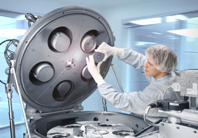
The new facility will feature a sputtering chamber that can carry out a wide range of PVD-coating processes. This enables trial-sized substrates with an edge length of a few centimeters to be coated. The clean room is used to analyze the sample substrate, and check if the electric conductivity is correct, if the thickness, optical properties and adhesiveness are right, and to see what internal stresses the coating is subject to.
Plansee says that it will develop and improve its coatings products for areas of application such as TFT flat screens, thin-film solar cells, large area and optical coating as well as coatings for data storage, and hard-material coatings for machining tools.


