
Researchers at Valencia University (UV) in Spain says that they have modified the photoconductance of nanoparticles of tungsten oxide (WO3) in a controlled manner.
Photoconductance is an optical and electrical phenomenon whereby a material becomes a better electrical conductor after absorbing light, while inverse photoconductance (IPC) describes materials that become less conductive after being exposed to light, the researchers say. This phenomenon has potential applications in the development of photonic and non-volatile memory devices and could be used to create new types of sensors that can be adjusted for different spectral properties.
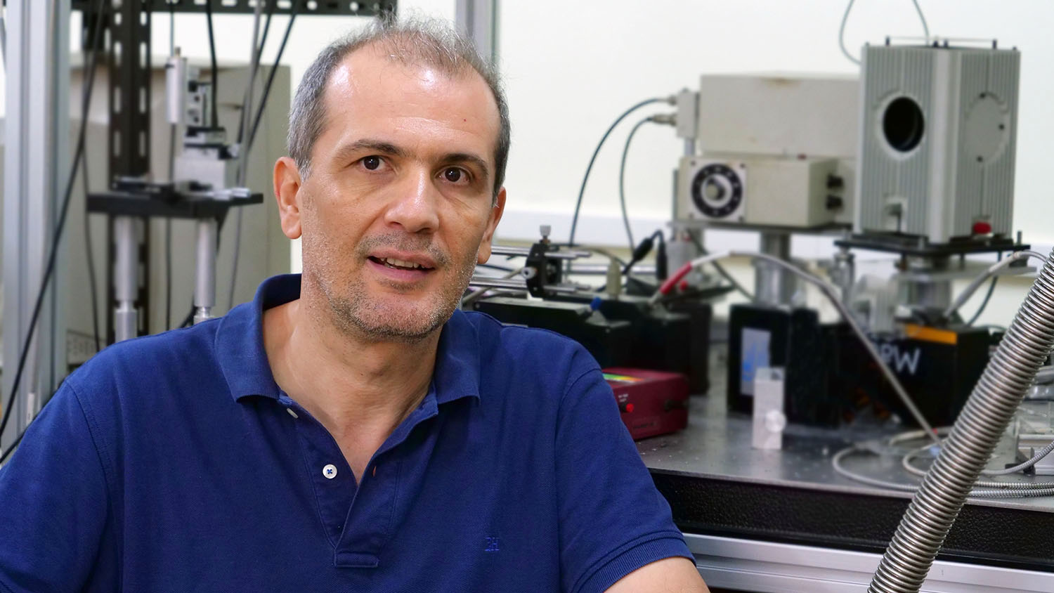
The research group led by Daniel Errandonea has managed to control and modify inverse photoconductance in a hybrid material based on nanoparticles of tungsten oxide with an excess of negative charges (type n), covered by a layer of copper oxide (CuO) with an excess of positive charges (type p). They have done this by subjecting the material to high pressures by using a device called diamond cell.
The results have been published in Advanced Science.
This story uses material from the University of Valencia, with editorial changes made by Materials Today. The views expressed in this article do not necessarily represent those of Elsevier.


