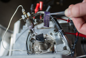
Using high-speed, thermally energized jets to deliver both precursor materials and inert gas, the research, performed at the Georgia Institute of Technology will focus on dramatically accelerating growth, improving the purity and increasing the aspect ratio of the 3D structures.
Known as focused electron beam-induced deposition (FEBID), the technique delivers a focused beam of high- energy electrons and an energetic jet of thermally excited precursor gases confined to the same spot on a substrate. Secondary electrons generated when the electron beam strikes the substrate cause decomposition of the precursor molecules, forming nanoscale 3D structures whose size, shape and location can be precisely controlled. This gas-jet assisted FEBID technique allows fabrication of high-purity nanoscale structures using a wide range of materials and combination of materials.
Overall, about two dozen materials have been successfully deposited using FEBID on different substrates, including semiconductors, dielectrics, metals and plastics. The researchers also plan to create nanostructures containing more than one material, allowing them to create unique properties not available in each individual material. Examples might include new types of ferromagnetic materials and photonic bandgap structures with unique properties.
By allowing the rapid atom-by-atom “direct writing” of materials with controlled shape and topology, the work could lead to a nanoscale version of the 3D printing processes now revolutionizing fabrication of structures at the macro scale. The technique could be used to produce nano-electromechanical sensors and actuators, to modify the morphology and composition of nanostructured optical and magnetic materials to yield unique properties, and to engineer high-performance interconnect interfaces for graphene and carbon nanotube-based electronic devices.
“This unique nanofabrication approach opens up new opportunities for on-demand growth of structures with high aspect ratios made from high-purity materials,” said Andrei Fedorov, the project’s leader and a professor in the George W Woodruff School of Mechanical Engineering at the Georgia Institute of Technology. “By providing truly nanoscale control of geometries, it will impact a broad range of applications in nanoelectronics and biosensing.”
The three-year US$660,000 grant is intended to help researchers develop a fundamental understanding of how the process works, accelerate the rate of materials growth and provide improved control over the process. The research will include both theoretical modelling and experimental evaluation.
The FEBID technique will likely not be used for high-volume fabrication because the process is difficult to scale up, Fedorov said. Accelerating the deposition rate will allow more rapid fabrication, but the 3D structures will still need to be produced one at a time. A partial solution to the scale-up challenge lies in the use of multiple electron beams and precursor jets operating in parallel.


