
Technologies supported at the new Enthone facility include the company’s MICROFAB bump wafer processes and ViaForm wafer deposition electrodeposition technologies, including damascene copper, through silicon via (TSV), copper redistribution layer (RDL), copper post, and lead-free bump applications.
“Taiwan represents over 65% of the world’s semiconductor foundry manufacturing, as well as 60% of the world’s semiconductor packaging market,” said Raymond Fong, vice president and managing director–Enthone Asia. “The center is strategically located to further support and collaborate with these world leaders on new and emerging technologies as they advance their product portfolio, and implement higher performance, more cost-effective wafer manufacturing throughout the Asia-Pacific region and across the globe.”
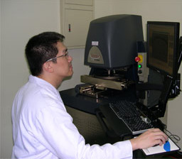
The center is staffed by Enthone’s team of applications experts and is designed to accommodate the stringent needs of the semiconductor market. Currently, the center provides wafer sample plating and testing for process optimization, bath composition analysis, and characterization of plated features and deposits for bump height, morphology, post-reflow inspection, alloy composition, thin film thickness, and SEM cross-sectioning for filling.
“The Enthone Semiconductor Applications Center provides our team of applications engineers and R&D chemists a unique opportunity to partner with our customers, while gathering critical feedback to validate and further optimize their manufacturing process.” said Michael Corey, global business director–Enthone Electronic Materials Group.

