
Smartphones that don't scratch or shatter. Metal-free pacemakers. Electronics for space and other harsh environments. These could all be made possible thanks to a new ceramic welding technology developed by a team of engineers at the University of California (UC) San Diego and UC Riverside.
The process, reported in a paper in Science, uses an ultrafast pulsed laser to melt ceramic materials along their interface and fuse them together. It works in ambient conditions and uses less than 50 watts of laser power, making it more practical than current ceramic welding methods that require heating the parts in a furnace.
Ceramics are fundamentally challenging to weld together because they need extremely high temperatures to melt. This means exposing them to extreme temperature gradients that can cause cracking, explained senior author Javier Garay, a professor of mechanical engineering and materials science and engineering at UC San Diego, who led the work in collaboration with UC Riverside professor and chair of mechanical engineering Guillermo Aguilar.
Ceramic materials are of great interest because they are biocompatible, extremely hard and shatter resistant, making them ideal for biomedical implants and protective casings for electronics. However, current ceramic welding procedures are not conducive to making such devices.
"Right now, there is no way to encase or seal electronic components inside ceramics because you would have to put the entire assembly in a furnace, which would end up burning the electronics," Garay said.
The engineers’ solution was to aim a series of short laser pulses along the interface between two ceramic parts, so that heat builds up only at the interface and causes localized melting. They call their method ultrafast pulsed laser welding.
To make it work, the researchers had to optimize two aspects: the laser parameters (exposure time, number of laser pulses and duration of pulses) and the transparency of the ceramic material. With the right combination, the laser energy couples strongly to the ceramic, allowing welds to be made using low laser power (less than 50 watts) at room temperature.
"The sweet spot of ultrafast pulses was two picoseconds at the high repetition rate of one megahertz, along with a moderate total number of pulses. This maximized the melt diameter, minimized material ablation and timed cooling just right for the best weld possible," Aguilar said.
"By focusing the energy right where we want it, we avoid setting up temperature gradients throughout the ceramic, so we can encase temperature-sensitive materials without damaging them," Garay said.
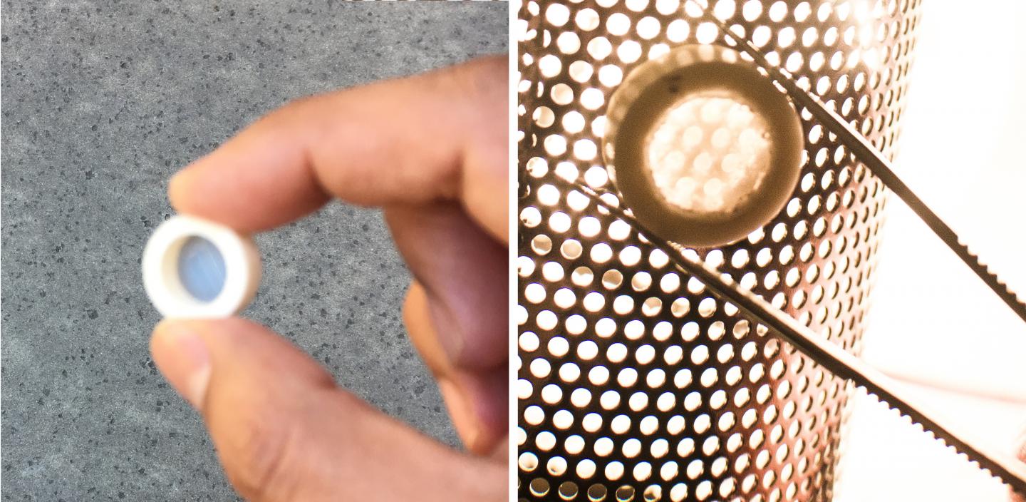
As a proof of concept, the researchers welded a transparent cylindrical cap to a ceramic tube. Tests showed that the welds are strong enough to hold a vacuum.
"The vacuum tests we used on our welds are the same tests that are used in industry to validate seals on electronic and optoelectronic devices," said first author Elias Penilla, who worked on the project as a postdoctoral researcher in Garay's research group at UC San Diego.
The process has so far only been used to weld small ceramic parts that are less than 2cm in size. Future plans will involve optimizing the method for larger scales, as well as for different types of materials and geometries.
This story is adapted from material from the University of California, San Diego, with editorial changes made by Materials Today. The views expressed in this article do not necessarily represent those of Elsevier. Link to original source.

